Photochemical etching is a subtractive, non-traditional machining process that uses chemical and photographic techniques to design and shape metal workpieces. After developing the design of the image on the workpiece, a strong chemical solution is poured over the workpiece. As a result, the workpiece corrodes selectively and removes all unnecessary material from areas that are not protected, leaving a sharp image or flawless part. Read More…
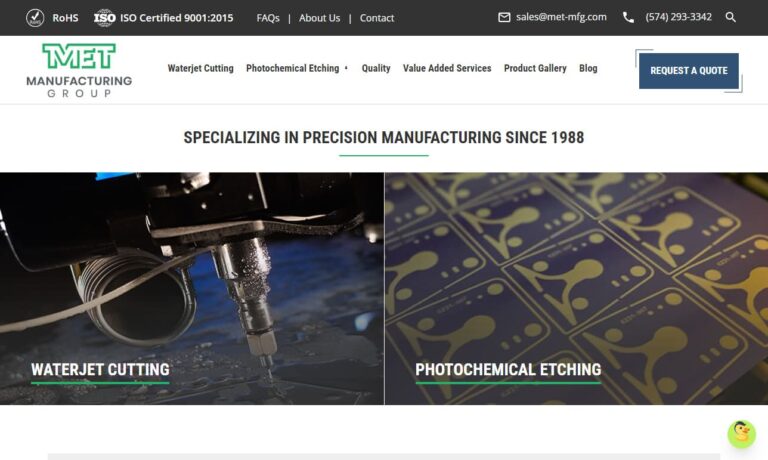
The MET Manufacturing Group, LLC process offers many technical & financial advantages in manufacturing various flat metal components. Try this precision etching, non-mechanical process for competitively priced, burr & stress free sheet metal products, up to 62 mil (.062”) thick. Our photo-chemical machining process is also known as photo-fabrication, photo etching, chemical milling & acid...
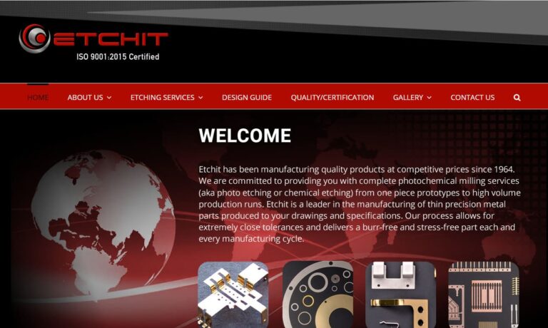
Etchit is your high-quality solution for custom-manufactured precision metal parts and components. We use photochemical machining to make products for such industries as aerospace, audio, automotive, computer, circuit board, decorative and fastener. Does your product need photo etching processes?
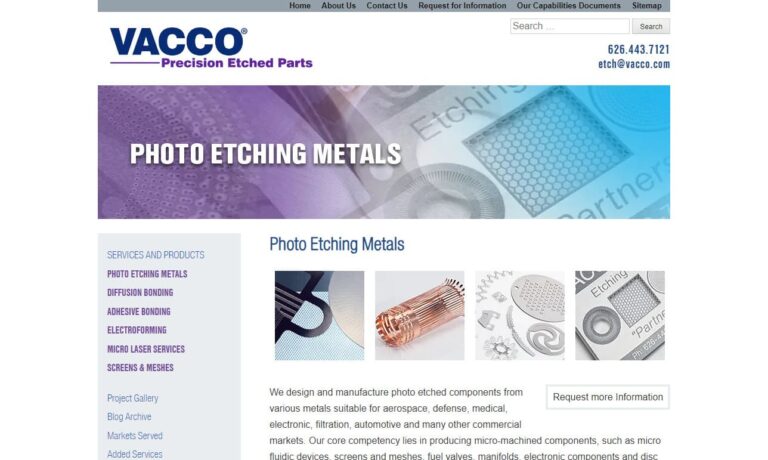
VACCO is the industry leader of Photo Chemical Etching of metal & polyimide components and devices. We specialize in Stainless steel, Titanium, and Copper, but work with a variety of different materials. We have over 60 years of experience in Chem Etching, and we offer Micro Laser Cutting & Welding, and Diffusion & Adhesive Bonding services along with an extensive range of value-added services. ...
Great Lakes Engineering is a trend setting manufacturer of surface mount stencils, precision laser cut parts, and photo chemical etched parts. We work with a wide range of materials, including Stainless Steel, Copper, Titanium, Nitinol, Nickel, Kovar and many others.

More Photo Etching Companies
What is Photochemical Etching?
Photochemical etching, also known as photo etching or chemical etching, is an advanced subtractive manufacturing process used to fabricate high-precision metal components. This technique utilizes photographic methods and photoresist imaging to selectively remove or preserve areas of metal, resulting in extremely intricate and accurate patterns that are challenging or impossible to create using traditional machining methods like stamping, laser cutting, or wire EDM.

The primary advantage of the photochemical machining (PCM) process is its ability to manufacture and produce precision metal parts with exceptional levels of detail, tight tolerances, and complex geometries. These can range from ultra-thin meshes and micro-components to larger flat parts—applications where burr-free edges and stress-free manufacturing are critical.
Photo etching creates thin and flat metal parts, with thicknesses starting from about ten microns (0.01 mm). This capability makes photo etching ideal for industries that require fine metal etching and microfabrication, such as electronics, aerospace, medical devices, and automotive engineering.

The Photochemical Etching Process
The photochemical etching process—sometimes referred to as chemical milling or photochemical machining—is a highly controlled, multi-step procedure that enables the creation of intricate and complex features in a wide range of metals and alloys. Its unmatched flexibility and design freedom make it a preferred choice for prototyping, small-batch production, and even high-volume manufacturing of precision metal parts.

Step-by-Step Overview of the Photochemical Etching Workflow
-
Design & Photo Tool Plotting
The process begins with the creation of a phototool—a photographic negative of the desired pattern or profile. Engineering design software (such as CAD) is used to develop the artwork, which is then transferred onto a photographic film to form the phototool. This master pattern defines the areas to be etched and those to be protected during the chemical process.
-
Material Preparation
The chosen metal sheet or substrate is cut to size and meticulously cleaned to remove any surface contaminants (such as dirt, grease, oil, or rust) that could hinder photoresist adhesion. Cleaning methods include mechanical scrubbing and chemical cleaning, with the latter—often involving mild pickling and degreasing agents—being preferred for minimizing surface damage.
-
Photoresist Application
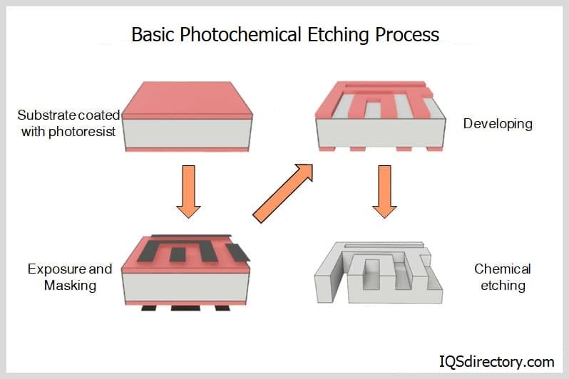
A light-sensitive photoresist material is uniformly coated onto the metal surface. This thin organic layer is formulated to withstand etching chemicals while accurately transferring the phototool’s pattern via exposure to ultraviolet (UV) light.
-
Soft Bake
The coated metal is gently heated to evaporate residual solvents in the photoresist, preventing bubbles and ensuring a defect-free layer for precise imaging.
-
Alignment & UV Exposure
For multi-layered or double-sided etching, precise alignment of the phototool is critical. The photoresist-coated substrate is exposed to UV light through the phototool, causing the photoresist to become either soluble (positive resist) or insoluble (negative resist) in the developer solution, depending on the resist type.
-
Development
The exposed metal is immersed in a developer solution, which washes away the soluble photoresist, leaving the desired pattern protected and the rest of the surface exposed for chemical etching.
-
Chemical Etching
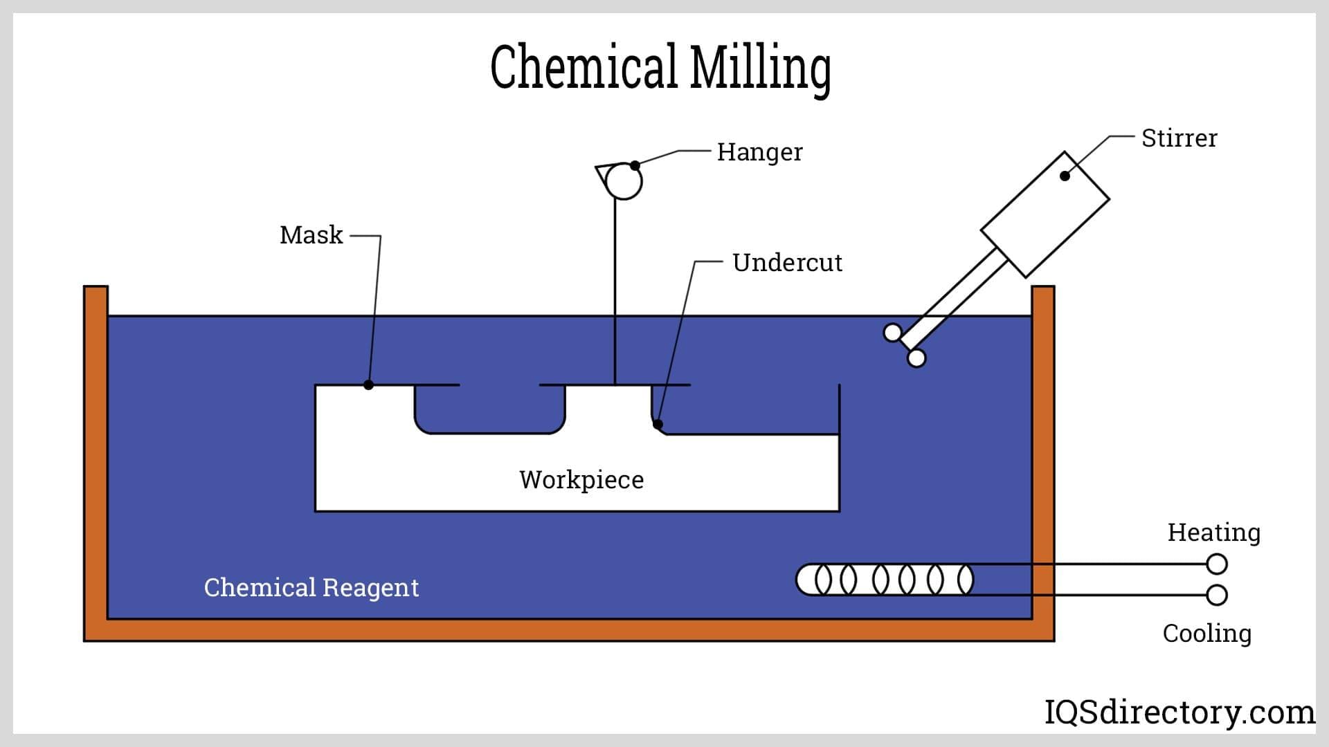
The substrate is placed in an etchant bath (commonly ferric chloride or cupric chloride for metals such as stainless steel, copper, or nickel alloys). The etchant selectively dissolves the exposed regions, precisely replicating the phototool pattern in the metal. Etch time, temperature, and agitation are tightly controlled for optimal results.
-
Photoresist Removal & Stripping
Once etching is complete and the desired metal features have been created, the remaining photoresist is stripped away using solvents or oxygen combustion, yielding the finished photochemically etched component.
Photo Tool Plotting: Key Considerations
The accuracy of the phototool is fundamental to achieving tight tolerances in photo etched parts. Factors affecting phototool dimensions include:
- Temperature and Humidity Variations: Changes in environmental conditions can cause dimensional shifts in the phototool material. Controlled environments and thicker polyester films help to maintain consistency. In advanced applications, laser direct writing is employed for ultimate precision.
- Etch Factor: The ratio of lateral etching (undercut) to etch depth is critical. Most etchants act isotropically, meaning they etch in all directions, leading to undercuts beneath the protective photoresist. Accurate process control is needed, especially for deep etches.
Material Preparation: Ensuring Surface Integrity
Proper preparation of the workpiece is essential for high-quality photochemical machining. The metal surface must be free from contaminants to ensure uniform photoresist adhesion and consistent etching results. Two main cleaning procedures are used:
- Chemical Cleaning: Involves pickling the metal in a solution containing degreasing agents and mild acids. This method provides thorough cleaning with minimal mechanical damage, making it the preferred choice for delicate or high-precision components. Learn more about chemical machining companies.
- Mechanical Cleaning: Employs scrubbing and mild degreasing agents to physically remove contaminants. While effective, this method can slightly abrade the surface and is generally reserved for less sensitive applications.

Photoresist Coating: Types and Importance
Photoresists are specialized organic materials that play a crucial role in transferring intricate patterns onto metal substrates. During photoresist coating, a uniform layer is applied to the cleaned metal, which is then dried and readied for exposure. Photoresists offer strong resistance to etching solutions, ensuring that only the intended areas are removed.
Photoresists are classified as:
- Positive Photoresists: Become soluble in the developer solvent upon exposure to UV light, allowing those areas to be washed away.
- Negative Photoresists: Become chemically resistant (insoluble) after exposure, so unexposed areas are removed by the developer.
Choosing the correct photoresist type depends on the specific application, desired resolution, and etching chemistry. For high-resolution microfabrication, positive resists are often preferred due to their superior edge definition.
Soft Bake: Optimizing the Photoresist Layer
Soft baking is a controlled heating process that evaporates residual solvents from the freshly coated photoresist layer. This critical step prevents defects such as bubbling or delamination, which can compromise feature accuracy during exposure and development. Optimal soft bake parameters (time and temperature) are determined based on the resist formulation and substrate type.
Alignment and Exposure: Achieving Pattern Precision
For multi-layered or double-sided etching, precise alignment of the phototool is essential to ensure accurate registration between layers. Exposure involves projecting UV light through the phototool onto the photoresist-coated substrate. The duration, wavelength, and intensity of exposure are calibrated based on material thickness, resist type, and feature resolution.
After exposure, the substrate is developed to reveal the patterned resist, followed by a hard bake to further solidify the resist and enhance etch resistance. Nitrogen blow drying and rinsing with distilled water are used to clean the surface before etching.
The Etching and Stripping Process: Revealing the Final Part
During the chemical etching step, the developed substrate is immersed in an etchant bath tailored to the specific metal alloy. Common etchants include ferric chloride (for stainless steel, nickel, and copper), nitric acid, and cupric chloride. The etchant removes the exposed metal while the protected areas remain intact, producing the intended component geometry.
Once etching is complete, photoresist stripping is performed to remove all remaining resist material. This can be achieved using solvents, plasma ashing, or oxygen combustion, depending on the resist type and substrate material. The finished part is then thoroughly cleaned and inspected for quality assurance.

Photochemical Etching Applications and Advantages
Photochemical etching is widely used in industries demanding high-precision metal components, fine features, and design flexibility. Whether you are researching how photo etching is used in aerospace, evaluating suppliers for electronics manufacturing, or comparing the benefits of chemical etching versus laser cutting, understanding its diverse applications and advantages can help inform your purchasing decisions.
Key Applications of Photochemical Etching

- Aerospace Components: Lightweight, high-strength parts such as fuel filters, EMI/RFI shielding, and micro-meshes.
- Gaskets and Seals: Custom-shaped, burr-free gaskets and precision metal seals for engines and industrial equipment.
- Fine Filters and Screens: Micro-perforated screens, sieves, and filtration elements for medical, scientific, and industrial use.
- Decorative Applications: Intricate metal nameplates, badges, jewelry, and custom branding elements.
- Printed Circuit Boards (PCBs): Prototyping and small-batch production of circuit patterns and flexible circuits.
- Electronics: Lead frames, connectors, shielding, and micro-electromechanical systems (MEMS) components.
- Medical Grade Materials: Precision surgical instruments, implantable device components, and diagnostic tools with biocompatible metals.
- Automotive Industry: Fuel injector parts, sensor components, and intricate interior trim elements.
- Optical and Photonics: Apertures, masks, and alignment targets for lasers and imaging systems.
- Energy Sector: Battery current collectors, fuel cell plates, and microfluidic channels.
Advantages of Photochemical Etching Over Alternative Processes
- Reduced Production Time: Rapid prototyping and short lead times compared to stamping or machining.
- Cost Efficiency: No expensive tooling required; phototools are inexpensive to produce and modify, making the process ideal for both small and large production runs.
- High Precision and Complexity: Capable of producing complex, burr-free features with tight tolerances, including ultra-fine geometries and micro-holes.
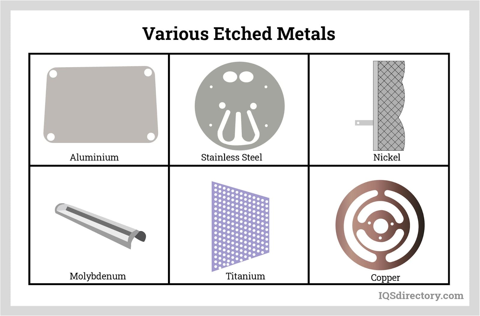
- Material Versatility: Works with a wide range of metals and alloys, including stainless steel, copper, nickel, titanium, aluminum, and precious metals.
- No Mechanical Stress: The non-contact chemical process avoids the introduction of mechanical stresses, deformation, or work hardening—critical for sensitive or thin components.
- Scalability and Design Freedom: Quick design changes and scalable production volumes, from prototypes to mass manufacturing, with minimal additional cost.
- Burr-Free and Clean Edges: Eliminates the need for secondary finishing operations, saving time and cost.
- Environmentally Friendly Options: Modern etching facilities utilize recycling and waste treatment systems to minimize environmental impact.
When Should You Use Photochemical Etching?
Are you wondering whether photochemical etching is right for your next project? This process is ideal if you require:
- Complex patterns or micro-features that are difficult to achieve with traditional CNC machining, stamping, or laser cutting.
- Rapid prototyping with fast turnaround times and low tooling costs.
- Flat, thin, and burr-free metal parts for sensitive applications.
- High repeatability and precision for mass production or critical industries.
- Stress-free manufacturing of delicate, brittle, or thin materials.
For a more in-depth comparison of photochemical etching and alternative metal fabrication methods, visit our Chemical Machining Guide.
Factors to Consider When Selecting a Photochemical Etching Service Provider
Choosing the right photochemical etching company can significantly impact the quality, lead time, and overall success of your project. Consider these decision factors when comparing suppliers:
- Material Compatibility: Confirm the provider’s experience with your required metal or alloy (e.g., stainless steel, copper, nickel silver, titanium, etc.).
- Feature Resolution and Tolerance: Evaluate the company’s capability to achieve your desired feature sizes and tolerances—especially important for microfabrication and ultra-fine patterns.
- Production Capacity: Ensure the supplier can meet your volume needs, whether it’s rapid prototyping or large-scale manufacturing.
- Quality Assurance: Look for ISO certifications, in-process inspection, and post-etching quality control procedures.
- Value-Added Services: Some vendors offer additional services such as forming, plating, heat treating, or assembly.
- Lead Times and Flexibility: Ask about typical turnaround times, responsiveness to design changes, and support for custom projects.
- Environmental Compliance: Inquire about waste management, chemical recycling, and compliance with environmental regulations.
Choosing the Right Photochemical Etching Company
To ensure the best results when sourcing photochemically etched components or precision metal parts, it is recommended to compare several photochemical etching suppliers. Our Photochemical Etching Directory allows you to:
- Browse business profiles that highlight each supplier’s areas of expertise, process capabilities, and certifications.
- Use our patented website previewer to quickly compare offerings and specializations from leading photochemical etching manufacturers worldwide.
- Contact multiple suppliers directly using our streamlined RFQ (Request for Quote) form to obtain competitive pricing and lead times.
- Read customer testimonials and case studies to evaluate the provider’s reputation and track record in your industry.
Ready to find a photochemical etching partner for your application? Explore our supplier directory and submit your project requirements today.
Frequently Asked Questions About Photochemical Etching
How does photochemical etching compare to laser cutting or stamping?
Photochemical etching offers superior precision for fine features, no burrs or mechanical deformation, and lower setup costs for small to medium volumes. Unlike stamping, there are no expensive hard tools, and unlike laser cutting, there is no heat-affected zone, making it ideal for thin and intricate parts.
Which metals can be photo etched?
Commonly photo etched metals include stainless steel, copper, nickel, titanium, aluminum, brass, silver, and even some hard-to-machine alloys. Each metal requires tailored etchants and process parameters for optimal results.
What is the minimum feature size achievable with photochemical etching?
Feature sizes can be as small as 25 microns (0.025 mm), depending on the metal thickness, photoresist quality, and process control. Photochemical etching is ideal for micro-scale components and intricate geometries.
How do I request a quote or sample?
To request a quote, simply complete our online RFQ form and upload your drawings or specifications. Our network of qualified suppliers will respond with competitive proposals tailored to your needs.
Summary: The Value of Photochemical Etching in Modern Manufacturing
Photochemical etching provides unmatched capabilities for producing precision metal parts with complex designs, fine features, and stress-free manufacturing. Its applications span industries from aerospace and medical devices to electronics and automotive, offering numerous benefits over alternative metal fabrication methods. By understanding the process, its advantages, and the key factors in supplier selection, you can make informed purchasing decisions that drive innovation and efficiency in your manufacturing projects.


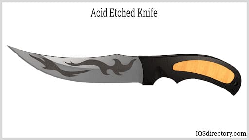
 Broaching
 CNC Machining
 Expanded Metals
 Laser Cutting
 Metal Etching
 Metal Fabrication
 Perforated Metals
 Screw Machine Products
 Metal Stampings
 Sheet Metal Fabrication
 Tube Fabrication
 Water Jet Cutting
 Castings & Forgings
 Bulk Material Handling
 Electrical & Electronic Components
 Flow Instrumentation
 Hardware
 Material Handling Equipment
 Metal Cutting Services
 Metal Forming Services
 Metal Suppliers
 Motion Control Products
 Plant & Facility Equipment
 Plant & Facility Supplies
 Plastic Molding Processes
 Pumps & Valves
 Recycling Equipment
 Rubber Products & Services